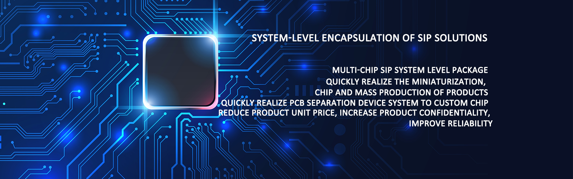
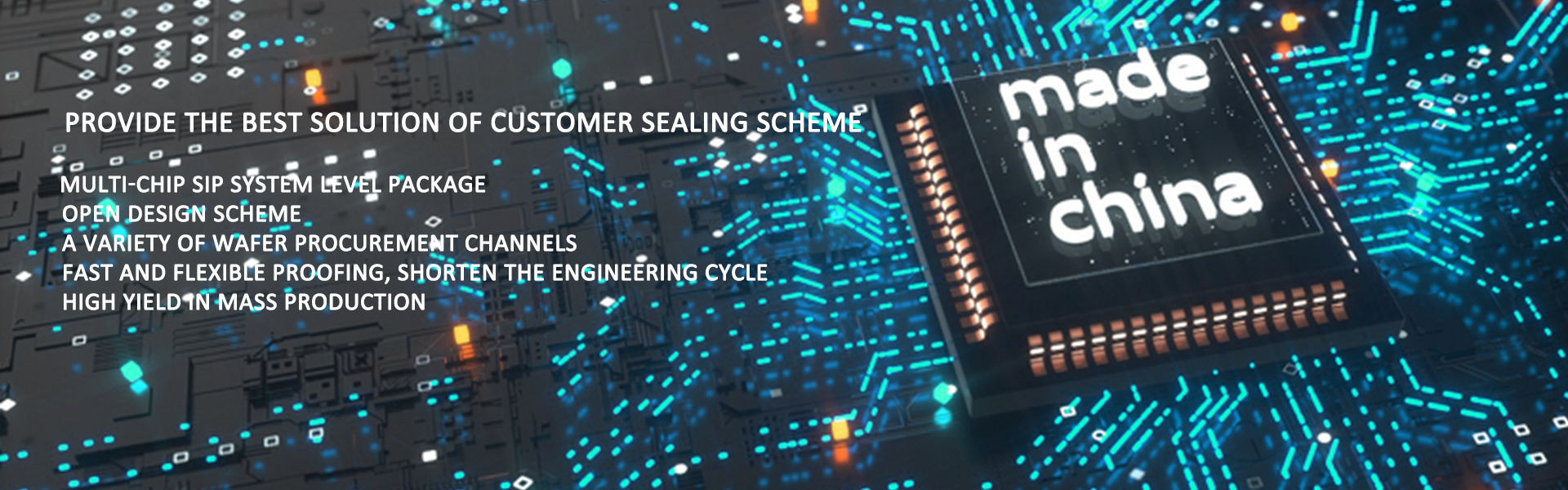
As shown in the figure below, covering different processes from wafer testing to AOI testing, we can provide customers with fast sampling and small-scale mass production services.

According to the process, it can be divided into three stages: the front stage, the middle stage, and the back stage.
(1) The previous process includes wafer testing, wafer thinning, and cutting, which includes both CP testing of IC wafers, full and half cutting of wafers; This also includes CV testing of MEMS wafers and laser stealth cutting. For wafer thinning, the grinding followed by cutting or semi cutting followed by grinding process can be selected based on the type and thickness requirements of the wafer to be processed. Please refer to the solution section for details
(2) The intermediate process includes passive component installation, positive assembly of active chips, lead bonding, flip flopping, bottom filling, and other processes. Specifically, it involves high-density SMT mounting, regular and fine pitch flip flop processes, 2.5D/3D chip stacking, and the selection of CUF and MUF. Please refer to the solutions section for details.
(3) The subsequent processes include plastic sealing, laser marking, electromagnetic shielding process, BGA ball planting, cutting, AOI testing, and other processes. The specific design includes full plastic sealing and selective plastic sealing, cavity shielding and conformal shielding, fully automatic and manual ball planting, regular and irregular cutting, etc., as detailed in the solution section.